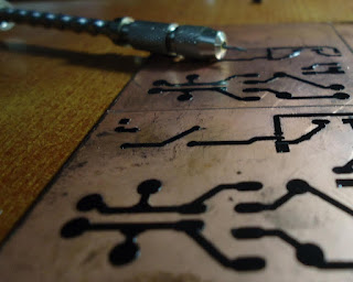
While making PCB's at home isn't particularly difficult, If you've done any kind of building at all, you can appreciate how much difference it makes to stuff a pre-printed PCB versus hand wiring on bread board or GPB.
All you Need is:
First of all software I use to design the PCBs is Protel DXP, or you can use EAGLE PCB. Protel DXP is not Free ware, you have to purchase the licence to use that.
EAGLE is free, put out by CadSoft.You can download for free either for a Linux or Windows version of this layout tool, whose only limitation is a maximum of one schematic page and about a 2.5x4" PCB size.
All you Need is:
- PCB Designing Software
- Simple Copper Plated PCB Cost: RS 100 Max
- Nearest Computerized Car Number Plate Maker..!! Cost: Can be any 50-500 RS.
- Etching Solution Cost: Rs.90 per 500GMS
- Water
- Container
- Small Hand Drill Cost Rs.150
First of all software I use to design the PCBs is Protel DXP, or you can use EAGLE PCB. Protel DXP is not Free ware, you have to purchase the licence to use that.
EAGLE is free, put out by CadSoft.You can download for free either for a Linux or Windows version of this layout tool, whose only limitation is a maximum of one schematic page and about a 2.5x4" PCB size.
For the demostration I'm going to show you simple bridge circuit, with Protel DXP.
Now,
Make the Schematic file in the Protel DXP but putting components in the schematic capture,connect each components and after adding PCB to the project, I will import that whole schematic in to the PCB.
Now the PCB Viewer is opened, and arrange the components and route the whole PCB using Auto routing.
Now what to have to do is,Go to File> Print out the PCB file using the virtual PDF installed on you machine and save it to the .PDF flie.
STEPS TO MAKE IT HARD:
- After printing this file to the .PDF format, convert that file to .JPEG using Adobe Photoshop(PS) also do it "X - Mirror" in PS. Save it as .JPEG. Take this .JPEG file and the perfect size of your PCB file in mm (That can be done be CTRL+M in Protel DXP) to the nearest Computerized Car Number Plate maker.
Making it X-Mirror is very important as you have whole track in the bottom layer. - Give this JPEG file and let him cut through his computerized Plotter on a thick sticker and stick that sticker to your copper plated PCB.
- See how my circuit looks like.(I have used another circuit down here, but yours will be nearly same)
- Etching Safety Precautions :
- Wear Hand glows while putting/taking out circuit in/from solution, as the solution heats up too much when you add FeCl3 in to water, and also can harm your skin.
- The solution you have to use is FeCl3(two table spoons for small size PCB) + some hot water(not too much!!), which is used in the laboratories. It will not be a nightmare if you disliked the Chemistry..!! (sorry have taken another different image, picture is just to demonstrate you the process of making PCB, FYI : it's from my LAB only, not copied from the internet.!!).Put it in this solution for whole day in one container.

After putting it in the Etching Container for whole day, take it out, wash your circuit and peel off that sticker.
This is the image after the whole process.
Drill the holes at your desired places. Mount the components.
Enjoy Electronics...!!!


7 comments:
Good efforts. step by step PCB making method. Useful for electronic students.
I want to add some tips:
You can use a laser printer, some shiny paper magazine and an iron, to make the transfer to the pcb. (all allmost free)
Then, for the removing copper part you can use HCL + H2O2 (bath cleaner and oxygened water) instead of FeCl3, it's safer and can be dropped to the sewer. The reaction is slower than with FeCL3 but this is a bonus when you are making your own PCBs for first time, if you want to make the reaction faster, you can either increase the concentration of H2O2 or increase the temperature. To stop the reaction just clean your PCB with tap water.
Greatings from Chile!
And keep designing..
One commonly used method of making a PCB is that of photo etching. Through photo etching, you can create a complicated circuit for an electrical device by exposing a laminate copper board to UV light and transferring the circuit design directly onto the board. It's a quick way to create a PCB for use. Thanks a lot.
Thanks for such an informative article and the extensive explanation.This is really a helpful for the newbies..Great job done keep it up..http://www.rushpcb.co.uk/Assembly/MixedAssemblyPlacement.aspx
Could you please get me a copper clad board? I'm ready to pay for it including courier charges...
you can easily get Copper clad board from your nearest electronics and industrial parts distributor shop.it costs around 100-150..according to size.
Thanks Rushi for your reply... But unfortunately none of the Electronics Distributors in Kolkata is ready to sell a single piece! They would only sell in bulk quantities!
Post a Comment