Search

Friday 24 August 2012

Alan Turing's life and legacy : A Salute


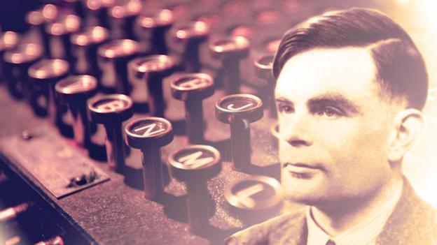
Alan Mathison Turing was an English mathematicianlogiciancryptanalyst, andcomputer scientist. He was highly influential in the development of computer science, giving a formalisation of the concepts of "algorithm" and "computation" with the Turing machine, which can be considered a model of a general purpose computer.Turing is widely considered to be the father of computer science and artificial intelligence.

During World War II, Turing worked for the Government Code and Cypher School (GCCS) at Bletchley Park, Britain's codebreaking centre. For a time he was head of Hut 8, the section responsible for German naval cryptanalysis. He devised a number of techniques for breaking German ciphers, including the method of the bombe, an electromechanical machine that could find settings for the Enigma machine
.

This bombsight mechanical computer was used on board Lancaster and other aircraft in the Second World War. It was used to aim the bombs, taking factors such as aircraft height and speed and weather conditions into account. Unlike electronic computers, which are programmed using software, mechanical computers carried out their computations according to the physical shape and design of the mechanism. The gears, linkages and cams literally embodied the equations that needed to be solved.

After the war he worked at the National Physical Laboratory, where he created one of the first designs for a stored-program computer, the ACE. In 1948 Turing joined Max Newman's Computing Laboratory at Manchester University, where he assisted in the development of the Manchester computers.


The Pilot ACE was one of the first computers built in the United Kingdom, at the National Physical Laboratory (NPL) in the early 1950s.
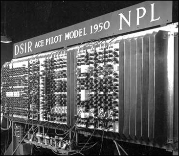
It was a preliminary version of the full ACE, which had been designed by Alan Turing. After Turing left NPL (in part because he was disillusioned by the lack of progress on building the ACE), James H. Wilkinson took over the project, Harry Huskey helped with the design. The Pilot ACE ran its first program on May 10, 1950 and was demonstrated to the press in December 1950.
Codebreaker is an exhibition developed by the Science Museum to celebrate the centenary of the birth of this pioneering British figure.
At the heart of the exhibition is the Pilot ACE computer, built to Turing’s ground-breaking design. It is the most significant surviving Turing artefact in existence.
Alongside this remarkable machine is a sequence of exhibits showcasing Turing’s breadth of talent. Together with interactive exhibits, personal recollections and a wealth of historic imagery, the exhibition offers an absorbing retrospective view of one of Britain’s greatest twentieth-century thinkers.
GoogleThis exhibition was made possible with the generous support of Google.
Alan Turing I salute your centenary. Where would the world be without your work and as the father of Computer Science.
References:
  1. History of Computing in the Twentieth Century" edited by Gian-Carlo Rota et al, Academic Press (1980).
  2.  J.H.Wilkinson, "Rounding Errors in Algebraic Processes", reprinted by Dover (1994).
  3. Sciencemuseum.org
  4. Agar, Jon (2003). The government machine: a revolutionary history of the computer. Cambridge, Massachusetts: MIT Press

Monday 20 August 2012

A Small Project for "Newbies" : Fun Stuff : Bi-stable Multivibrator

Introduction


This is the circuit of the Bi-stable Multivibrator. Either transistor can be on while the other is off, and the circuit will retain its state until it is changed by an external signal or power is turned off. Thus, this circuit represents the simplest possible binary memory. In this experiment, you will construct and demonstrate such a circuit.

Schematic Diagram

If, when power is first applied, Q1 turns on, its output will be a logic 0. This will be applied to Q2's input resistor, keeping Q2 turned off so that its output will be a logic 1. This logic 1 will be applied back to Q1's input resistor, keeping Q1 turned on and holding the entire circuit locked into this stable state.


On the other hand, if Q1 stays off at power-up, it will apply a logic 1 to Q2's input, thus turning Q2 on. The resulting logic 0 output from Q2 will in turn hold Q1 off. The circuit will then remain in this stable state indefinitely.

This circuit is a bistable multivibrator, or flip-flop. Push "set" input at right switch to bring the output high (5V). Push the "reset" input at lower right to bring the output low (ground). 

The transistors are cross-coupled in such a way that the circuit has two stable states. Initially, Q2 is on and Q1 is off. Since Q1 is off, no current is flowing through it, and its collector voltage is close to 5V. This allows current to flow through into the base of Q2, which keeps Q2 switched on. Q2 is in saturation mode, keeping the collector voltage close to ground; this prevents any current from flowing into the base of Q1 to switch it on. 

If you push the "set" input momentarily, this provides base current to Q1, switching it on, bringing its collector low, which stops the base current flowing to Q2. So the circuit switches to the opposite state. Pushing the "reset" input switches back.

Because this circuit has two possible logical states, it is known technically as a multivibrator. Because it has two possible stable states, it is a bistable multivibrator. It is also the most basic possible binary latch circuit. In the next few experiments we'll look at ways to expand this circuit and modify its behavior. But first, we'll examine the operation of this basic circuit.


Here is the Simulation of Astable Multivibrator which is derived from internet, But the similarly this circuit will swithover LEDs after pressing the push buttons simultaneously in Bi-stable Multivibrator.

This is for example only, do not consider resistance values, voltage supplies, etc., the first figure is correct for this project.


Parts List

To construct and test the bistable multivibrator circuit on your breadboard, you will need the following experimental parts:

    • (6) 1K, ¼-watt resistors (brown-black-red). 
    • (2) 330E, ¼-watt resistors (brown-black-red). 
    • (2) BC547 or 2N4124 NPN silicon transistors.
    • (2) Mini Push Button Switches 
    • (2)LEDs Green, Red 
    • 5V Power Supply Adapter.
    • White wire or existing jumpers. 
    • Black wire or existing jumpers. 

Monday 13 August 2012

Arduino Leonardo AVR Development Board

Arduino Leonardo AVR Development Board
Arduino Leonardo AVR Development Board is a microcontroller board based on the Atmel ATmega32u4. It offers 20 digital IOs (of which 7 can be used as PWM outputs and 12 as analog inputs), a 16MHz crystal oscillator, a micro USB connection, a power jack, an ICSP header, and a reset button. The Leonardo differs from all preceding boards in that the ATmega32u4 has built-in USB communication, eliminating the need for a secondary processor. This allows the Leonardo to appear to a connected computer as an HID, such as a mouse or keyboard, in addition to a virtual (CDC) serial / COM port. The Leonardo board contains everything needed to support the microcontroller. Simply connect it to a computer with a USB cable or power it with an AC-to-DC adapter or battery to get started.

Specifications

Microcontroller: ATmega32u4
Operating voltage: 5V
Input voltage (recommended): 7-12V
Input voltage (limits): 6-20V
Digital I/O pins: 20
PWM channels: 7
Analog input channels: 12
DC current per I/O pin: 40mA
DC current for 3.3V pin: 50mA
Flash memory: 32Kb (ATmega32u4)
of which 4Kb is used by bootloader
SRAM: 2.5Kb (ATmega32u4)
EEPROM: 1Kb (ATmega32u4)
Clock speed: 16MHz
------------------------------------****

Here is one Hack that will give you example of extension if the application of the Leonardo.

The newly released Arduino Leonardo has a few very interesting features, most notably the ability to act as a USB keyboard and mouse.. This feature isn’t exclusive to the Leonoardo, as Michael explains in a build he sent in – the lowly Arduino Uno can also serve as a USB HID keyboard with just a firmware update.
The Arduino Uno (and Mega) communicate to your computer through a separate ATmega8U2 microcontroller. Simply by uploading new firmware with the Arduino Device Firmware Upgrade, it’s easy to have your old Arduino board gain some of the features of newer boards such as the Teensy or Leonardo.
Michael goes through the steps required to make this upgrade work and ends his build by showing off an Arduinofied ‘cut, copy and paste’ button project as well as a few multimedia controls. You can check those builds out in the video after the break.
If emulating a USB keyboard isn’t your thing, it’s also possible to install LUFA firmware to emulate everything from joysticks to USB audio devices. Very cool, and very useful.

Courtesy:
www.hackaday.com

Wednesday 1 August 2012

Introduction to Raspberry Pi : "Take a Byte"


Raspberry Pi Logo.svgThe Raspberry Pi is a credit card sized single-board computer developed in the UK by the Raspberry Pi Foundation with the intention of stimulating the teaching of basic computer science in schools.
The Raspberry Pi has a Broadcom BCM2835 system on a chip (SoC), which includes an ARM1176JZF-S 700 MHz processor,VideoCore IV GPU, and 256 megabytes of RAM. It does not include a built-in hard disk or solid-state drive, but uses an SD card for booting and long-term storage.
Available two versions Priced at US$ 25 and US$ 35.
The Foundation provides Debian and Arch Linux ARM distributions for download. Also planned are tools for supporting Python as the main programming language, with support for BBC BASIC, (As "Brandy Basic", the BBC BASIC clone), C, and Perl.

RaspberryPi.jpgHARDWARE:

Initial sales are of the Model B, with plans to release the Model A sometime later. Model A has one USB port and no Ethernet controller, and will cost less than the Model B with two USB ports and a 10/100 Ethernet controller.
Though the Model A doesn't have an RJ45 Ethernet port, it can connect to a network by using a user-supplied USB Ethernet or Wi-Fi adapter. There is in reality no difference between a model A with an external Ethernet adapter and a model B with one built in, because the Ethernet port of the model B is actually a built-in USB Ethernet adapter. As is typical of modern computers, generic USB keyboards and mice are compatible with the Raspberry Pi.
File:Raspberrypi block function v01.svgThe Raspberry Pi does not come with a real-time clock, so an OS must use a network time server, or ask the user for time information at boot time to get access to time and date for file time and date stamping. However, a real-time clock (such as the DS1307) with battery backup can be added via the I2C interface.

Operating Systems

This is a list of operating systems running, ported or in the process of being ported to Raspberry Pi
  • Multi-purpose light distributions:
    • Squeezed Arm Puppy, a version of Puppy Linux (Puppi) for the ARMv6 (sap6) specifically for the Raspberry Pi.

What’s a Raspberry Pi?

The Raspberry Pi is a credit-card sized computer that plugs into your TV and a keyboard. It’s a capable little PC which can be used for many of the things that your desktop PC does, like spreadsheets, word-processing and games. It also plays high-definition video. We want to see it being used by kids all over the world to learn programming.

What’s the difference between Model A and Model B?


Model A has 128Mb of RAM
 Model A has been redesigned to have 256Mb RAM, one USB port and no Ethernet (network connection). Model B has 256Mb RAM, 2 USB port and an Ethernet port.

What are the dimensions of the Raspberry Pi?

The Raspberry Pi measures 85.60mm x 53.98mm x 17mm, with a little overlap for the SD card and connectors which project over the edges. It weighs 45g.

What SoC are they using?

The SoC is a Broadcom BCM2835. This contains an ARM1176JZFS, with floating point, running at 700Mhz, and a Videocore 4 GPU. The GPU is capable of BluRay quality playback, using H.264 at 40MBits/s. It has a fast 3D core accessed using the supplied OpenGL ES2.0 and OpenVG libraries.

Why did they select the ARM11?

Cost and performance.

How powerful is it?

The GPU provides Open GL ES 2.0, hardware-accelerated OpenVG, and 1080p30 H.264 high-profile decode.
The GPU is capable of 1Gpixel/s, 1.5Gtexel/s or 24 GFLOPs of general purpose compute and features a bunch of texture filtering and DMA infrastructure.
That is, graphics capabilities are roughly equivalent to Xbox 1 level of performance. Overall real world performance is something like a 300MHz Pentium 2, only with much, much swankier graphics.

Will it overclock?

There’s a little overclocking headroom – most devices will run happily at 800MHz. There’s no BIOS per se, but we do support booting bare metal code, so something could be done.

Can we add extra memory?

No. The RAM is a POP package on top of the SoC, so it’s not removable or swappable.

Is sound over HDMI supported?

Yes.

Is there a GPU binary?

Yes. The GPU binary also contains the first stage bootloader.

Can we add a touchscreen?

We haven’t experimented with any touchscreens yet, but there’s no electronic reason why it shouldn’t work. There’s lots of discussion about this on the forums. The main issue people are encountering seems to be one of cost; touchscreens are very pricey!

Wednesday 18 July 2012

Build a digital spirit level using a SCA610 accelerometer

A bubble or spirit level meter is a handy tool to find whether a surface is horizontal or vertical. It is often carried by civil engineers, mechanical engineers, surveyors, carpenters, and many other professionals whose work involve precise alignments of horizontal and vertical planes. Original spirit levels had two banana-shaped curved glass vials at each viewing point and were much more complicated to use. Mechanical spirit level meters are still available both in 1D and 2D formats. However at present time their electronic counterparts have also emerged and are even available in modern Android equipped cell phones.. Here’s a demo of such an electronic spirit level made by using a Microchip PIC16F684 micro, a SCA610 accelerometer and a handful of other discrete components.

Digital spirit level meter
Theory
The heart of this project is the SCA610 accelerometer IC that senses the inclination of a surface. Bases on VTI 3D MEMS technology, SCA610 is a very reliable, accurate and stable one-axis analog accelerometer. It requires a single power supply and provides an analog output voltage proportional to the inclination. According to its datasheet, if the device is powered with a precise +5.0V, the analog output voltages for +1g (vertical), 0g (horizontal), and -1g (vertical in opposite direction) inclinations would be 3.75V, 2.50V, and 1.25V, respectively. Voltages between 1.25V and 3.75V are linearly interpolated and mapped to the inclination angles varying from +90° to -90°. The analog signal can be processed by a microcontroller through an ADC channel to retrieve the inclination information.
Circuit diagram
The microcontroller used in this project is PIC16F684 which has just enough I/O pins and a built-in 10-bit A/D converter required for this project. The microcontroller runs at 8.0 MHz using the internal oscillator. The SCA610 sensor output goes to AN0 ADC channel of PIC16F684. The microcontroller takes quick multiple ADC samples which are averaged for a better estimation of inclination angle. There are five LEDs connected to RC0 through RC4 port pins and they are arranged in a row. Based on the direction of inclination the LEDs run in either forward or in reverse direction. There is a buzzer connected to RC5 pin which beeps continuously until the entire board settles at 0g or horizontal position. The buzzer used in the circuit is a ON/OFF type. What that means is it turns on when the RC5 pin goes high. If the device is aligned perfectly horizontal then only a central blue LED flashes and the buzzer mutes.


The axis direction of the SCA610 accelerometer is marked on the chip, as shown in the circuit diagram above.

Circuit setup on a breadboard
Software
The firmware for this project has been written in C using mikroElektronika’s mikroC Pro for PIC compiler. Note that the buzzer used in this project is a high impedance ON/OFF type and the software just turns the RC5 pin high in order to make the buzzer on. So this firmware won’t drive a buzzer that requires an ac signal. You can download the source code and compiled HEX output of the firmware from the following link.

Download

This project used a one-axis accelerometer chip and therefore, the alignment can be measured in only one direction at a time. However, the concept can be extended for simultaneous measurements of orientation in two dimensions by adding one more SCA610 sensor or just choosing a dual axis accelerometer (like ADXL202).

Courtesy : Embedded Lab

Wednesday 27 June 2012

Taking a dump from some old hardware


NYC Resistor shows you how to have some fun with electronics from the junk bin.Their post called The Joy of Dumping encourages you to look around for older memory chips and see what they’ve been hiding away for all these years.
I found this post when I was searching some stuff for my project work.
The targets of their hunt are EPROM chips. Note the single ‘E’. These are Erasable Programmable Read-Only Memory chips, and predate EEPROM which adds “Electrically” to the beginning of the acronym.  You used to use a UV light source to erase the older types of memory. In fact we’ve seen some EPROM erasers as projects from time to time. These shouldn’t be too hard to find as they were prevalent as cheap storage back in the 1980′s.
If the quartz window on the top of the chips has been shielded from ambient UV light, you should still be able to read them and it’s as easy as hooking up your Arduino. Is it useful? Not really, but it still can be neat to interface with what might otherwise never make its way back out of the junk box.

Thursday 14 June 2012

Wireless Temperature Sensor

There are many ways to achieve this. One of the simplest ways is to use a voltage to frequency conversion chip along with an analog temperature sensor such as LM335 or a thermistor, and then transmit the modulated frequency signal via an RF data link module. Alternatively, we can use a digital temperature sensor and sending the sensor readings over RF serial data link digitally. In this post I will stick with the first approach.


The following schematic shows the circuit design:
Here the 1/4 LM324 (or LM2902) forms a voltage follower to buffer the input voltage from the resistor-thermistor voltage divider, and the divider output is fed into an LM331 voltage to frequency converter. The LM331 portion of the circuit was taken directly from the reference design.
The capacitor at pin 5 needs to be adjusted so that the maximum frequency output from the oscillator is below the maximum bit rates supported by the RF link. The RF data transmitter I used has a maximum bit rate of 2400 bps and thus I used a 47nF capacitor and the oscillation frequency is around 700 Hz under room temperature.
The frequency output from LM331 is again buffered via another 1/4 LM324 (or LM2902) before feeding into the RF data link transmitter. This voltage to frequency circuit is arguably not the most accurate one and you could improve your accuracy by adding an op-amp integrator as illustrated in the datasheet, but for the temperature measurement application we are discussing here, this simple circuit is accurate enough.
According to the LM331 data sheet, the timing components need to have very high stability in order to achieve a high level of accuracy and minimize frequency drift. The picture above shows the finished transmitter portion of the temperature sensor. Note that the power supply must be regulated in order to obtain accurate readings since it is referenced by the thermistor voltage divider.
I could have built the receiver using another LM331 as a frequency to voltage converter and use the voltage readouts to calculate the temperature readings. But then I would need to use an A/D converter to convert the signal back to digital form in order to perform the calculation. To simplify the design, I used an Arduino MCU (ATmega328) to measure the frequency output from the RF data link receiver directly. The following picture shows the setup on the receiver end.
The oscilloscope capture below shows the output waveform from the receiver when the transmitter side is under room temperature.
With the transmitter and receiver working, now we need to convert the received frequency readings back to the temperature readings. Again, to help you understand how the calculation is done I have included the reference schematic below:
Reference Design

We know that the converter’s output frequency is a linear function of the input voltage at the voltage divider:
f=C0RntcRntc+R0Vcc=C1RntcRntc+R0
C0 is a constant that can be derived from the following equation according to the datasheet:
C0=Rs209RLRtCt
Since the temperature is roughly inversely proportional to the thermistor value within a small temperature range:
1RntcT
We can further simplify the frequency output to:
f=C11+C2T
And thus we can derive the measured temperature as:
T=C1fC21C2
Although the two constants C1 and C2 can be determined by the theoretical values of the components, it is probably simpler to obtain them experimentally by measuring two or more frequencies at different temperature points.
Below is the Arduino code I used. The FreqCounter library I used can be found here. Note that parameters in the code are tailored specifically for the type of thermistor I used and they are also affected by the transmitter supply voltage (in my case the transmitter operates on 5V). You will need to re-calculate the parameters based on the equations I gave above.


#include 
unsigned long frq;
float a = -165.0;
float b = 151735.0;
float GetTemp(float f)
{
  return a + (b/f);
}
void setup()
{
  Serial.begin(9600);
}
void loop()
{
    FreqCounter::f_comp = 106;
    FreqCounter::start(1000);
    while (FreqCounter::f_ready == 0)
        frq = FreqCounter::f_freq;    
    Serial.println(GetTemp(frq));
}