This I2C tutorial shows you how the I2C protocol works at the physical
bit level. It only discusses single master mode (a single controlling
device) as this is the most common use for I2C in a small system.

SDA : Serial Data
SCL : Serial Clock
I2C Tutorial : Typical SDA and SCL signals

I2C Tutorial : Instruction sequence data from
master to slave
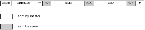
A master device sends the sequence S ADDR W and then waits for an acknowledge bit (A) from the slave which the slave will only generate if its internal address matches the value sent by the master. If this happens then the master sends DATA and waits for acknowledge (A) from the slave. The master completes the byte transfer by generating a stop bit (P) (or repeated start).
I2C Tutorial : Instruction sequence data from slave
to master

A similar process happens when a master reads from the slave but in this case, instead of W, R is sent. After the data is transmitted from the slave to the master the master sends the acknowledge (A). If instead the master does not want any more data it must send a not-acknowledge which indicates to the slave that it should release the bus. This lets the master send the STOP or repeated START signal.
I2C Tutorial : START (S) and STOP (P) bits.
I²C (pronounced
I-squared-C) created by
Philips Semiconductors and commonly written as 'I2C' stands for
Inter-Integrated Circuit and allows communication of data between I2C
devices over two wires. It sends information serially using one line
for data (SDA) and one for clock (SCL).
Master and slave
The phillips I2C protocol defines
the concept of
master and slave devices. A master device is simply the device that is
in charge of the bus at the present time and this device controls the
clock and generates START and STOP signals. Slaves simply listen to the
bus and act on controls and data that they are sent.
The master can send data to a slave
or receive data from a slave - slaves do not transfer data between
themselves.
Multi Master
Multi master operation is a more
complex use of
I2C that lets you have different controlling devices on the same bus.
You only need to use this mode if you have more than one
microcontroller on the bus (and you want either of them to be the bus
master).
Multi master operation involves
arbitration of
the bus (where a master has to fight to get control of the bus) and
clock synchronisation (each may a use a different clock e.g. because of
separate crystal clocks for each micro).
Note: Multi master is not
covered in this I2C tutorial as the
more common use of I2C is to use a single bus master to control
peripheral devices e.g. serial memory, ADC, RTC etc.
Data and Clock
The I2C interface uses two
bi-directional lines
meaning that any device could drive either line. In a single master
system the master device drives the clock most of the time - the master
is in charge of the clock but slaves can influence it to slow it down
(See Slow Peripherals below).
The two wires must be driven as open
collector/drain outputs and must be pulled high using one resistor each
- this implements a 'wired AND function' - any device pulling the wire
low causes all devices to see a low logic value - for high logic value
all devices must stop driving the wire.
Note : If you use I2C you
can not put any other (non I2C)
devices on the bus as both lines are used as clock at some point
(generation of START and STOP bits toggles the data line). So you can
not do something clever such as keeping the clock line inactive and use
the data line as a button press detector (to save pins).
You will often will find devices
that you realise
are I2C compatible but they are labelled as using a '2 wire interface'.
The manufacturer is avoiding paying royalties by not using the words
'I2C'!
There are two wires (three if you
include ground!) :
I2C Turorial: Signals definition
SCL : Serial Clock
I2C Turorial: end of signal definition
Speed
Standard clock speeds are 100kHz and
10kHz but
the standard lets you use clock speeds from zero to 100kHz and a fast
mode is also available (400kHz - Fast-mode). An even higher speed
(3.4MHz - High-speed mode) for more demanding applications - The mid
range PIC won't be up this mode yet!
Note that the low-speed mode has
been omitted (10kHz) as the standard now specifies the basic system
operating from 0 to 100kHz.
Slow peripherals
A slow slave device may need to stop
the bus
while it gathers data or services an interrupt etc. It can do this
while holding the clock line (SCL) low forcing the master into the wait
state. The master must then wait until SCL is released before
proceeding.
Data transfer sequence
A basic Master to slave read or
write sequence for I2C follows the following order:
I2C Tutorial : I2C basic command sequence.
- 1. Send the START bit (S).
- 2. Send the slave address (ADDR).
- 3. Send the Read(R)-1 / Write(W)-0 bit.
- 4. Wait for/Send an acknowledge bit (A).
- 5. Send/Receive the data byte (8 bits) (DATA).
- 6. Expect/Send acknowledge bit (A).
- 7. Send the STOP bit (P).
I2C Tutorial : end of I2C basic command sequence.
Note: You can use 7 bit
or 10 bit addresses.
The sequence 5 and 6 can be repeated
so that a multibyte block can be read or written.
Data Transfer from master to slave
A master device sends the sequence S ADDR W and then waits for an acknowledge bit (A) from the slave which the slave will only generate if its internal address matches the value sent by the master. If this happens then the master sends DATA and waits for acknowledge (A) from the slave. The master completes the byte transfer by generating a stop bit (P) (or repeated start).
Data transfer from slave to master
A similar process happens when a master reads from the slave but in this case, instead of W, R is sent. After the data is transmitted from the slave to the master the master sends the acknowledge (A). If instead the master does not want any more data it must send a not-acknowledge which indicates to the slave that it should release the bus. This lets the master send the STOP or repeated START signal.
Device addresses
Each device you use on the I2C bus
must have a
unique address. For some devices e.g. serial memory you can set the
lower address bits using input pins on the device others have a fixed
internal address setting e.g. a real time clock DS1307. You can put
several memory devices on the same IC bus by using a different address
for each.
Note: The maximum number
of devices is limited by the number
of available addresses and by the total bus capacitance (maximum 400pF).
General call
The general call address is a
reserved address
which when output by the bus master should address all devices which
should respond with an acknowledge.Its value is 0000000 (7 bits) and
written by the master 0000000W. If a device does not need data from the
general call it does not need to respond to it.
I2C Tutorial : Reserved addresses.
0000 000 1 START byte - for slow micros without I2C
h/w
0000 001 X CBUS address - a different bus protocol
0000 010 X Reserved for different bus format
0000 011 X Reserved for future purposes
0000 1XX X Hs-mode master code
1111 1XX X Reserved for future purposes
1111 0XX X 10-bit slave addressing
0000 001 X CBUS address - a different bus protocol
0000 010 X Reserved for different bus format
0000 011 X Reserved for future purposes
0000 1XX X Hs-mode master code
1111 1XX X Reserved for future purposes
1111 0XX X 10-bit slave addressing
I2C Tutorial : End of reserved addresses.
Most of these are not that useful
for PIC microcontrollers except perhaps the START byte and 10 bit
addressing.
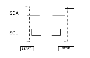
START (S) and STOP (P) bits
START (S) and STOP (P) bits are
unique signals that can be generated on the bus but only
by a bus master.
Reception of a START bit by an I2C
slave device
resets its internal bus logic. This can be done at any time so you can
force a restart if anything goes wrong even in the middle of
communication.
START and STOP bits are defined as
rising or falling edges on the data line while the clock line is kept
high.
I2C Tutorial : text definition of START and STOP signals
| START condition (S) | SCL = 1, SDA falling edge |
| STOP condition (P) | SCL = 1, SDA rising edge |
I2C Tutorial : end of text definition of START and STOP signals
The following diagram shows the
above information graphically - these are the signals you would see on
the I2C bus.
I2C Tutorial : end of definition of START and STOP signals
I2C Tutorial : end of definition of START and STOP signals
Note : In a single master
system the only difference between a
slave and a master is the master's ability to generate START and STOP
bits. Both slave and master can control SDA and SCL.
Repeated START (Sr)
This seems like a confusing term at
first as you
ask yourself why bother with it as it is functionally identical to the
sequence :
S ADDR (R/W) DATA A P
The only difference is that for a
repeated start
you can repeat the sequence starting from the stop bit (replacing the
stop bit with another start bit).
S ADDR (R/W) DATA A Sr
ADDR (R/W) DATA A P
and you can do this indefinitely.
Note: Reception of both S
or Sr force any I2C device reset its
internal bus logic so sending S or Sr is really resetting all the bus
devices. This can be done at any time - it is a
forced reset.
The main reason that the Sr bit
exists is in a
multi master configuration where the current bus master does not want
to release its mastership. Using the repeated start keeps the bus busy
so that no other master can grab the bus.
Because of this when used in a
Single master configuration it is just a curiosity.
Data
All data blocks are composed of 8
bits. The
initial block has 7 address bits followed by a direction bit (Read or
Write). Following blocks have 8 data bits. Acknowledge bits are
squeezed in between each block.
Each data byte is transmitted MSB
first including the address byte.
To allow START and STOP bit
generation by the
master the data line (SDA) must not be changed while the clock (SCL) is
high - it can only be changed when the clock is low.
Acknowledge
The acknowledge bit (generated by
the receiving
device) indicates to the transmitter that the the data transfer was ok.
Note that the clock pulse for the acknowledge bit is always created by
the bus master.
The acknowledge data bit is
generated by either
the master or slave depending on the data direction. For the master
writing to a slave (W) the acknowledge is generated by the slave. For
the master receiving (R) data from a slave the master generates the
acknowledge bit.
I2C Tutorial : Definition of ACK bits
| Acknowledge | 0 volts |
| Not acknowledge | High volts |
I2C Tutorial : End of definition of ACK bits
ACK data master --> slave
In this case the slave generates the
acknowledge signal.
When a not-acknowledge is received
by the bus
master the transfer has failed and the master must generate a STOP or
repeated START to abort the sequence.
ACK data slave --> master
In this case the master generates
the acknowledge signal.
Normally the master will generate an
acknowledge
after it has received data but to indicate to the slave that no more
data is required on the last byte transfer the master must generate a
'not-acknowledge'. This indicates to the slave that it should stop
sending data. The master can then generate the STOP bit (or repeated
START).
I2C Tutorial : Specifics for the 16F88
Pin configuration
To use the I2C mode in the 16F88 the
SDA and SCL
pins must be initialised as inputs (TRIS bit = 1) so that an open drain
effect is created. By setting them as inputs they are not driving the
wires and an external pull up resistor will pull the signals high.
Slave mode
The 16F88 fully implements all slave
functions except general call.
The general call function does not
really matter as it is quite specialised commanding all devices on the
bus to use some data.
A low output is generated by driving
the signal
line low and changing the pin direction to an output. A high output is
generated by changing the pin direction to an input so that the
external resistor pulls the signal high.
In slave mode this action is done
for you by the
SSP module (the outputs of the register at SDA and SCL are driven low
automatically - regardless of the state of the register value).
Master mode
Basically there is very limited
master mode functionality.
There are two elements that are
provided:
- Interrupts
- Pin control
16F88 Interrupts
There are two interrupts that
activate on
reception of either a START or STOP condition. These two interrupts are
only useful in a multi master mode system where it is necessary for the
non-master device to detect the start and stop conditions. So for a
single master system they are of no use at all!
16F88 Pin control
Note When the SSP module is active
SDA and SCL
output are always set at zero regardless of the state of the register
values. So all you have to do is control the port direction.
In master mode (16F88)
SDA and SCL must be controlled using software.
I2C Tutorial : Specifics for 16F877A
It does it all for you!
- Full master mode.
- Full slave mode.
- Full general call.
Note if you want a chip
with full master and slave mode
operation look for the MSSP module in a PIC chip e.g. 16F877A - then
you won't need more software - just enough to drive the module.